

PCB Fabrication


Half-holes pcb semi-hole
Item No.: H000125
Plate thickness / number of layers: 1.6MM/2 layer
Surface treatment: semi-hole immersion gold process
Minimum aperture: 0.2MM
Minimum line width, line spacing: 4/4 MIL
Surface treatment: semi-hole immersion gold process
Minimum aperture: 0.2MM
Minimum line width, line spacing: 4/4 MIL
Description
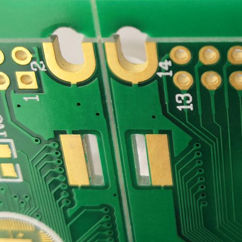
What are Plated Half-Hole/Semi-Hole?
Plated half-holes (or Semi holes) are predominantly used for board-on-board connections, mostly where two printed circuit boards with different technologies are combined. E.g. the combination of complex microcontroler modules with common, individually designed PCBs.Additional applications are display, HF or ceramic modules which are soldered to the base printed circuit board.
The board-on-board PCBs therefore need plated half-holes, which serve as SMD connection pads. Through directly connecting the PCBs together, the whole system is considerably thinner than a comparable connection with multi-pin connectors.
Manufacturing
Through setting back the copper shell from the conture, the plating is protected from mechanical damaging.
Therefore the plated half-holes can be milled precisely what strongly improves the process reliability.
Internal Half-holes are also producable.


Drawing

How to indicate castellated holes in your design?
Castellated hole design varies from software to software, but the end result in the Gerber files should be as follows. Please refer to the documentation of your chosen design software for more information.
Add a via or plated hole directly on the outline of the boards where the plated half hole is required. Ensure that half of the via is on the board and half is on the outside of the outline.
The following should be included:
- Copper layers (GTL and GBL): Copper pads on both top and bottom copper layers for each castellated hole.
- Solder mask layers (GTS and GBS): Solder mask openings on both sides.
- Drill layer (TXT/DRL): A drill hole for each castellated hole.
- Mechanical/Outline layer (GML/GKO): The outline should cross the drill hole.

Construction & Edge Feature Details
This PCB module includes plated semi‑holes or edge plate features along its PCB outline, allowing edge connections or landing pads at board borders. It is built on rigid FR‑4 substrate, with copper foil layers for signal and return paths. The board includes solder mask and silkscreen layers for protection and labeling. Edge plating or plating around the semi‑holes ensures electrical contact and mechanical robustness. This design aligns with pcb board design practices requiring edge connectivity and compatibility with other modules. Board edge finish, hole plating quality, and pad layout around the semi‑holes are specified in submitted design files. Because of the plating at edges, trace routing near board perimeter and solder mask clearances need careful layout, especially when ordering via pcb maker online platforms where file checks validate edge features.
Fabrication Process & Compatibility with Design Standards
Manufacture starts from customer’s design files (e.g. Gerber), including specified edge features / semi‑hole plating, board outline, and layer stack. After drilling if needed, plating is applied to the holes and edges, then solder mask and silkscreen are printed. Edge semi‑holes are milled or routed to shape after plating; copper plating ensures continuity and solderability. The design rules for pad annular rings, mask clearance, mechanical strength around plated edges are followed. Compatible with workflows of pcb layout services, enabling designers to include semi‑hole / half‑hole plating in their layouts. Quality control includes inspection of plating at edges, solder mask registration, and mechanical strength of edge features.
Intended Applications & User Profiles
This semi‑hole plated edge PCB module is suited for hardware engineers, industrial electronics designers, and OEMs needing board modules with edge connection points—e.g. modules to be soldered onto larger boards or to interface with edge connectors. Use within security panels, sensor modules, communication instrumentation, or control units where edge lands simplify mounting. Customers who work with pcb manufacturers or submit orders via pcb maker online systems will find this board type useful when module‑to‑board interfaces or mechanical assembly demand edge plated pads. It is rigid; not designed for flexing; usage assumed in rigid mounting or module integration environments.
Use Scenarios
Industrial Module Integration Environments
In settings producing sensor modules, communication daughter boards, or security accessory boards, rigid modules with plated semi‑holes allow integration at board edges. In assembly lines, modules may be soldered onto a mainboard along edge pads; these plated edges enable soldering without traditional connector hardware. pcb board design must account for mask clearance and edge routing so that these edge pads remain accessible and durable.
Prototype / Online Ordering Workflow
Designers upload layout with semi‑hole plated edges, define layer and edge plating specs, mask & silkscreen, copper weight. First prototypes verify pad alignment, plating continuity, and edge milled profiles. Feedback may adjust pad geometry or routing near edges. Ordering through pcb maker online or from pcb manufacturers, these boards allow module testing and validation before full deployment.
Mounted in Finished Products Requiring Edge Connectivity
Devices such as control panels, interface modules, or security system components often require connections at board edges for power, communication, or mounting. With plated semi‑holes, edge pads serve as direct connection points. This simplifies installation in enclosures, reduces connector space, and improves mechanical integration. Rigidity ensures the module does not deform under stress; protective finishes sustain electrical performance across temperature cycles and handling.

