

Single-double Sided PCB


Single Sided PCB Double Solder Mask
FR-4 1.6mm 1L 1Oz
Single Sided PCB Double Solder Mask
Single Sided PCB Double Solder Mask
Description
Single-Layer Structure with Dual Solder Mask Application
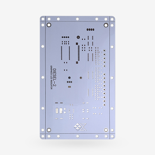
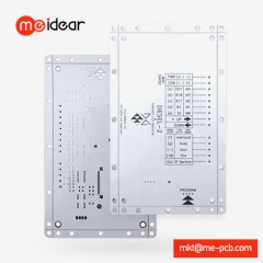
This product features a single-sided pcb circuit board design that is engineered for clarity, reliability, and ease of use during layout and assembly stages. The core structure is composed of a 1.6mm thick board layered with 1oz copper, which offers stable electrical performance for low-to-medium current applications. A unique attribute of this product is its green dual solder mask applied on both sides, ensuring precise masking even though circuitry is only present on one side. This design approach supports enhanced visual alignment and reduces the risk of solder bridging. As one of the versatile configurations offered by pcb fabrication companies, this board presents a clean and accessible platform for simplified routing and straightforward circuit board assembly in compact designs.
Material Choice and Surface Finish Compatibility
The board utilizes standard FR-4 glass epoxy substrate, known for its dimensional stability and insulation properties, making it a dependable choice in general-purpose electronics. The copper layer, with a standard 1oz weight, provides an appropriate balance of conductivity and thermal capacity for non-complex designs. With a green solder mask coating applied to both top and bottom surfaces, the product offers improved resistance to moisture, dust, and flux contamination during manufacturing. These construction elements match the performance expectations set by professional pcb manufacturing companies, ensuring that the board meets both quality and cost-efficiency targets. The material stack and finish compatibility support a range of manual and automated processes for circuit board assembly.
Manufacturing Specifications Supporting Layout Simplicity
Manufactured with a board outline tolerance of ±0.2mm and minimum hole size of 0.25mm, this single-sided PCB maintains consistent fabrication standards required for dependable layout execution. The mask application ensures that soldering zones are sharply defined, especially beneficial for novice or low-volume projects. As commonly used by entry-stage engineers or trial developers working with pcb prototype service providers, the simplicity of this board's routing allows for rapid prototyping and error-free component placement. Through its defined and repeatable dimensions, MEPCB delivers consistency aligned with the requirements of specialized pcb fabrication setups, supporting projects where design validation speed and mechanical accuracy are essential.
Product Advantages
Simplified Layer Design for Efficient Production
The single-layer configuration enables faster manufacturing cycles while reducing material complexity, making it suitable for rapid development needs. By including a dual solder mask, even in a single-sided setup, the board maintains visual symmetry and process compatibility for both manual and automated handling. This design is particularly beneficial to pcb fabrication companies producing high-mix, low-volume batches where simplified design and streamlined process control are key. The defined routing and limited interconnect depth allow users to test fundamental functions quickly, especially in early-stage pcb prototype service projects requiring minimal layers.
Stable Material and Precise Tolerances
Built with FR-4 epoxy material and 1oz copper, this board demonstrates reliable performance in temperature and mechanical stability. The ±0.2mm outline precision ensures fitment in fixed-size casings and fixtures used in downstream assembly. These attributes fulfill the expectations of pcb manufacturing companies that demand repeatability in limited-run applications. In addition, the 0.25mm hole dimension provides broad compatibility with standard connectors and through-hole parts, minimizing complications in circuit board assembly workflows. Overall, this construction promotes operational continuity while minimizing post-fabrication corrections.
Improved Assembly Alignment with Dual Solder Mask
Although designed with a single conductive layer, the dual green solder mask on both surfaces ensures that pad identification, alignment markings, and visual inspection during circuit board assembly are easier and more accurate. This characteristic supports quality control practices and reduces the chance of misalignment during manual soldering processes. For manufacturers that provide entry-level or custom board solutions, these enhancements align with the standards of reputable pcb fabrication companies and increase assembly efficiency. The board's visual clarity and material consistency contribute to lower rejection rates and more reliable prototype outcomes in small production runs.
Use Scenarios
Basic Electronic Device Prototyping
This single-sided board is suitable for use in fundamental prototyping efforts where simple signal pathways and essential component integration are needed. Developers working on low-complexity hardware can rely on its predictable electrical layout and minimal interference risk. The board’s standard FR-4 construction and uniform copper weight make it ideal for initial layout exploration. Often chosen by entry-level engineers and academic teams in collaboration with pcb prototype service providers, it facilitates a low-barrier entry into practical pcb circuit board evaluation and functional proof-of-concept testing.
Training-Oriented or Educational Environments
The combination of a single conductive layer and dual solder mask coating creates a visually clear and robust format for educational institutions and training programs. It supports repeated soldering practice without compromising structural integrity. Since the board includes standard hole sizes and defined spacing, it aids in instruction on component placement and basic circuit board assembly procedures. For technical schools and vocational centers sourcing materials through established pcb manufacturing companies, this board offers a consistent and low-risk format for teaching PCB fundamentals and manual assembly techniques.
Low-Volume Functionality Testing
For small development teams or boutique electronics firms focused on function-first evaluations, this board serves as a reliable base for single-purpose circuit tests. Its single-layer layout eliminates signal ambiguity, making debugging and iteration straightforward. The green solder mask ensures pad visibility under magnification or inspection lights. When collaborating with flexible pcb fabrication companies, such as MEPCB, teams can quickly source this configuration for pilot testing, component validation, or temporary deployment scenarios before migrating designs to multi-layer or production-grade builds through full-service pcb prototype service engagements.
About Us
MEPCB, founded in 2006, is a professional PCB manufacturer committed to serving global clients with comprehensive fabrication and assembly solutions. With over 18 years of industry experience, the company operates a 6,000-square-meter facility and employs more than 300 personnel. Its core services include PCB design, PCB fabrication, and circuit board assembly, covering product types from standard single and double-layer boards to HDI, aluminum, flexible, and high-frequency options. MEPCB is certified under ISO9001, ISO14001, and UL, demonstrating a strong emphasis on quality management and environmental compliance. The company serves clients across diverse industries by offering fast turnaround, competitive pricing, and strict production controls. Through continuous investment in process optimization and inspection systems, MEPCB has become a reliable partner for OEMs, startups, and other pcb manufacturing companies seeking dependable and scalable pcb prototype service.
FAQ
What type of substrate material is used for this PCB?
The board is made from FR-4 glass epoxy, offering strength and thermal stability in line with common PCB fabrication standards.
Is there copper on both sides of the board?
No, this is a single-sided board with copper only on one side, although both surfaces have a green solder mask.
What is the board thickness and copper weight?
The board is 1.6mm thick with 1oz copper on the conductive layer, matching standard pcb circuit board requirements.
Is the board suitable for pcb prototype service use?
Yes, its clear structure, defined mask areas, and single-layer design make it ideal for prototyping and layout testing.
Which companies commonly order this type of PCB?
It is often used by pcb manufacturing companies and educational clients that require simple, reliable boards for development or training.
Get reliable single-layer boards with dual solder mask from MEPCB—order now to support your next prototype or training project!

