

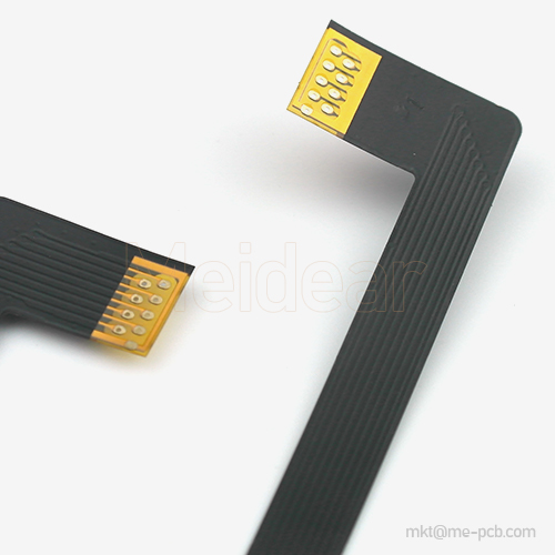


flexible FPC for medical device led lighting Camera cable
Item No.: F000128
Slim-profile flexible circuit for wearable gadgets, offering compact layout, durability in motion, and compatibility with pcb layout services and pcb maker online workflows.
Description
Compact Design and Material Structure
This flexible printed circuit board crafted for wearable electronics features a slim profile and lightweight construction to fit within compact device housings. The base material is flexible to accommodate bending, twisting, or movement associated with wearable device usage. Insulating layers cover conductive traces to prevent short circuits, corrosion, and wear from repeated motion. Trace width and spacing are designed to maintain signal fidelity even with minimal footprint. Connector pads are arranged to ease mounting and minimize bulk at interface points. These design decisions align with what customers expect from flex pcb solutions and reflect the capabilities of pcb manufacturers experienced in wearable‑grade electronics.
Electrical Reliability and Environmental Stability
Electrical pathways are engineered to support steady signal transmission, even under frequent movement or temporary deformation associated with wearable use. Proper insulation and coverlay materials are applied to resist moisture, sweat, and ambient environmental factors. The substrate and conductive patterns are laid out to avoid signal degradation over time. Thermal and electrical stresses are mitigated through material choice and layout planning. This level of reliability is essential for devices that are skin‑worn or subject to frequent flexing. Customers sourcing via pcb maker online channels receive a product fit for long‑term operation, while engineers performing pcb board design achieve high yield in wearable electronics assembly.
Manufacturing Process and Quality Assurance
Meidear applies processes such as precision copper patterning, lamination, and coverlay application in producing this flexible circuit board for smart wearable devices. Every board undergoes strict quality checks including visual inspection, dimensional accuracy, flex testing, and electrical continuity measurement. The production environment ensures that layout matches specifications for compact wearable circuits. Facilities support small to medium production volumes with the same attention to detail as prototypes. These capabilities meet the expectations of clients using pcb layout services and wanting consistent results from flexible circuit board vendors. Through controlled fabrication workflow and testing protocols, the finished product aligns with the needs of modern wearable device integration.
Product Advantages
Advantage One: Ultra‑Slim Profile for Wearable Integration
The board’s slim layer structure and minimal rigid areas allow integration into lightweight wearable devices without adding bulk. Flexible substrate and thin insulation layers enable wrapping or bending around curves, joints, or moving body parts. Signal paths maintain integrity despite flexing due to appropriately chosen materials and layout. This advantage is especially relevant in design environments where form factor constraints are tight, and performance cannot be sacrificed. Such thin‑profile design aligns with the expectations from flex board pcb requirements and is supported by Meidear’s production precision.
Advantage Two: Consistent Signal Transmission under Motion
Wearables often involve movement, bending, and sometimes physical stress. This flexible circuit board is engineered to maintain signal quality despite those dynamic conditions. Conductor layout, trace routing, and insulating coverlay work together to reduce risks of microfracture, intermittent connection, or noise introduced through flexing. Environment‑resistant materials help reduce impact from sweat or external moisture. The result is a wearable device circuitry component that remains reliable over many flex cycles. Those needing long lifespan wearable PCBs through pcb layout services will find this board meets those criteria.
Advantage Three: Fit for Small‑Scale and Custom Orders
Smart wearable projects often require low to medium volume, specific dimensions, and customized interface layouts. Meidear’s manufacturing supports such orders with precision copper patterning and layout flexibility. Connector pad positions, trace geometries, and insulating overlays can be adapted to the wearable design’s constraints. Customers ordering via pcb maker online or working with small batch prototyping benefit from this adaptability. This capacity for customization without compromising on function or reliability supports innovation in wearable technologies, aligning with expectations from both pcb manufacturers and designers of wearable electronics.
Use Scenarios
Everyday Wearable Health Devices
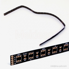
In wearable health monitors (such as fitness bands, heart‑rate sensors, or movement trackers), the flexible circuit board is positioned inside thin wristbands or form‑fitting enclosures. During production, the circuit layout is shaped to wrap around curved surfaces such as the underside of straps. Once assembled, frequent motion (flexing of the band at the wrist) demands that signal traces remain intact and that insulation holds up against sweat and slight moisture. Over time, reliable performance of the flex pcb inside health wearables supports accurate sensor readings and long battery life. This scenario is one where high quality pcb board design and robust flexible circuits are essential.
Smart Wearables Integrated into Apparel or Accessories
Applications like smart watches, glasses, smart clothing, or accessory‑embedded sensors embed flexible circuit boards within straps, frames, or fabric layers. Assembly during manufacturing often involves inserting the flexible board into housings, sewing or embedding into fabric, or connecting to small connectors for power or data. The durability of the flexible circuit board under mechanical stress, bending, and slight abrasion is critical. Users expect continuous performance even when garments move or accessories flex. The product’s design suits this kind of scenario, where compact layout and reliable flex capability are non‑negotiable.
Prototyping and Product Iteration for Wearable Tech
Early‑stage wearable device development involves testing multiple layout options, housing shapes, and connector placements. Engineers sourcing via pcb maker online or engaging pcb layout services need boards that accurately reflect final wearable dimensions and flex behavior. This flexible printed circuit board supports such prototyping by delivering consistent manufacturing and test validation (electrical continuity, flex endurance). Through iterations, design adjustments are made till fit, feel, and function meet requirements. Reliable components reduce redesign costs and support quicker time to device refinement.
About Us
Meidear manufactures flexible printed circuit boards tailored to wearable electronics and related compact applications. Its in‑house capabilities include flexible substrate processing, copper patterning, lamination, and application of coverlay layers. Quality control covers visual inspection, dimensional accuracy, flex endurance, and electrical continuity to ensure the boards meet required specifications. Support is provided for clients needing pcb layout services and those ordering through pcb maker online systems. Meidear operates production and prototyping with technical precision, delivering flexible components that maintain performance in motion and tight form factors while being reliable and manufacturable by established pcb manufacturers.
FAQ
What material properties make this product suitable for wearable devices and motion?
The material has flexible substrate, insulating coverlay, and trace routing optimized to endure repeated bending, minimal movement stress, and environmental exposure typical of wearable use.
How thin is this flexible circuit board and how does its compactness affect performance?
Sliding into tight enclosures is possible because the board is designed for low profile, minimal bulk while maintaining consistent signal paths, which is integral to good pcb board design and performance.
Can I use this with custom layout requests from pcb layout services?
Yes, Meidear supports specifying trace geometries, connector pad layouts, sensor pad positions, and layout constraints to match wearable device needs via professional layout services.
Is this product available to order online via pcb maker online channels?
Yes, ordering and quoting mechanisms are provided to deliver wearable‑grade flexible circuit board components through online inquiry and customization workflows.
How reliable is the flexible circuit board under sweat, moisture, and frequent flex in wearable applications?
The insulating coverlay, proper substrate choice, and rigorous flex testing help protect against moisture ingress, mechanical fatigue, and electrical degradation under regular wearable use.
Submit your wearable device PCB layout to request a custom flexible circuit board quote today!
This flexible printed circuit board crafted for wearable electronics features a slim profile and lightweight construction to fit within compact device housings. The base material is flexible to accommodate bending, twisting, or movement associated with wearable device usage. Insulating layers cover conductive traces to prevent short circuits, corrosion, and wear from repeated motion. Trace width and spacing are designed to maintain signal fidelity even with minimal footprint. Connector pads are arranged to ease mounting and minimize bulk at interface points. These design decisions align with what customers expect from flex pcb solutions and reflect the capabilities of pcb manufacturers experienced in wearable‑grade electronics.
Electrical Reliability and Environmental Stability
Electrical pathways are engineered to support steady signal transmission, even under frequent movement or temporary deformation associated with wearable use. Proper insulation and coverlay materials are applied to resist moisture, sweat, and ambient environmental factors. The substrate and conductive patterns are laid out to avoid signal degradation over time. Thermal and electrical stresses are mitigated through material choice and layout planning. This level of reliability is essential for devices that are skin‑worn or subject to frequent flexing. Customers sourcing via pcb maker online channels receive a product fit for long‑term operation, while engineers performing pcb board design achieve high yield in wearable electronics assembly.
Manufacturing Process and Quality Assurance
Meidear applies processes such as precision copper patterning, lamination, and coverlay application in producing this flexible circuit board for smart wearable devices. Every board undergoes strict quality checks including visual inspection, dimensional accuracy, flex testing, and electrical continuity measurement. The production environment ensures that layout matches specifications for compact wearable circuits. Facilities support small to medium production volumes with the same attention to detail as prototypes. These capabilities meet the expectations of clients using pcb layout services and wanting consistent results from flexible circuit board vendors. Through controlled fabrication workflow and testing protocols, the finished product aligns with the needs of modern wearable device integration.
Product Advantages
Advantage One: Ultra‑Slim Profile for Wearable Integration
The board’s slim layer structure and minimal rigid areas allow integration into lightweight wearable devices without adding bulk. Flexible substrate and thin insulation layers enable wrapping or bending around curves, joints, or moving body parts. Signal paths maintain integrity despite flexing due to appropriately chosen materials and layout. This advantage is especially relevant in design environments where form factor constraints are tight, and performance cannot be sacrificed. Such thin‑profile design aligns with the expectations from flex board pcb requirements and is supported by Meidear’s production precision.
Advantage Two: Consistent Signal Transmission under Motion
Wearables often involve movement, bending, and sometimes physical stress. This flexible circuit board is engineered to maintain signal quality despite those dynamic conditions. Conductor layout, trace routing, and insulating coverlay work together to reduce risks of microfracture, intermittent connection, or noise introduced through flexing. Environment‑resistant materials help reduce impact from sweat or external moisture. The result is a wearable device circuitry component that remains reliable over many flex cycles. Those needing long lifespan wearable PCBs through pcb layout services will find this board meets those criteria.
Advantage Three: Fit for Small‑Scale and Custom Orders
Smart wearable projects often require low to medium volume, specific dimensions, and customized interface layouts. Meidear’s manufacturing supports such orders with precision copper patterning and layout flexibility. Connector pad positions, trace geometries, and insulating overlays can be adapted to the wearable design’s constraints. Customers ordering via pcb maker online or working with small batch prototyping benefit from this adaptability. This capacity for customization without compromising on function or reliability supports innovation in wearable technologies, aligning with expectations from both pcb manufacturers and designers of wearable electronics.
Use Scenarios
Everyday Wearable Health Devices
In wearable health monitors (such as fitness bands, heart‑rate sensors, or movement trackers), the flexible circuit board is positioned inside thin wristbands or form‑fitting enclosures. During production, the circuit layout is shaped to wrap around curved surfaces such as the underside of straps. Once assembled, frequent motion (flexing of the band at the wrist) demands that signal traces remain intact and that insulation holds up against sweat and slight moisture. Over time, reliable performance of the flex pcb inside health wearables supports accurate sensor readings and long battery life. This scenario is one where high quality pcb board design and robust flexible circuits are essential.
Smart Wearables Integrated into Apparel or Accessories
Applications like smart watches, glasses, smart clothing, or accessory‑embedded sensors embed flexible circuit boards within straps, frames, or fabric layers. Assembly during manufacturing often involves inserting the flexible board into housings, sewing or embedding into fabric, or connecting to small connectors for power or data. The durability of the flexible circuit board under mechanical stress, bending, and slight abrasion is critical. Users expect continuous performance even when garments move or accessories flex. The product’s design suits this kind of scenario, where compact layout and reliable flex capability are non‑negotiable.
Prototyping and Product Iteration for Wearable Tech
Early‑stage wearable device development involves testing multiple layout options, housing shapes, and connector placements. Engineers sourcing via pcb maker online or engaging pcb layout services need boards that accurately reflect final wearable dimensions and flex behavior. This flexible printed circuit board supports such prototyping by delivering consistent manufacturing and test validation (electrical continuity, flex endurance). Through iterations, design adjustments are made till fit, feel, and function meet requirements. Reliable components reduce redesign costs and support quicker time to device refinement.
About Us
Meidear manufactures flexible printed circuit boards tailored to wearable electronics and related compact applications. Its in‑house capabilities include flexible substrate processing, copper patterning, lamination, and application of coverlay layers. Quality control covers visual inspection, dimensional accuracy, flex endurance, and electrical continuity to ensure the boards meet required specifications. Support is provided for clients needing pcb layout services and those ordering through pcb maker online systems. Meidear operates production and prototyping with technical precision, delivering flexible components that maintain performance in motion and tight form factors while being reliable and manufacturable by established pcb manufacturers.
FAQ
What material properties make this product suitable for wearable devices and motion?
The material has flexible substrate, insulating coverlay, and trace routing optimized to endure repeated bending, minimal movement stress, and environmental exposure typical of wearable use.
How thin is this flexible circuit board and how does its compactness affect performance?
Sliding into tight enclosures is possible because the board is designed for low profile, minimal bulk while maintaining consistent signal paths, which is integral to good pcb board design and performance.
Can I use this with custom layout requests from pcb layout services?
Yes, Meidear supports specifying trace geometries, connector pad layouts, sensor pad positions, and layout constraints to match wearable device needs via professional layout services.
Is this product available to order online via pcb maker online channels?
Yes, ordering and quoting mechanisms are provided to deliver wearable‑grade flexible circuit board components through online inquiry and customization workflows.
How reliable is the flexible circuit board under sweat, moisture, and frequent flex in wearable applications?
The insulating coverlay, proper substrate choice, and rigorous flex testing help protect against moisture ingress, mechanical fatigue, and electrical degradation under regular wearable use.
Submit your wearable device PCB layout to request a custom flexible circuit board quote today!

