HDI LED lighting PCB in Shenzhen China Mepcb
Views : 2210
Author : Meidear
Update time : 2024-08-08 09:31:04
In today's digital age, LED displays have become an indispensable element in fields such as information display, advertising, and event hosting. The key technology behind this visual feast is high-quality PCB boards. PCB, The PCB board of LED display is the "skeleton" of electronic products, while the PCB board of LED display is its "soul". In indoor and outdoor display screens, the application of 2-layer or 4-layer boards is the most common. Small pitch LED display screens use more layers of circuit boards to meet the needs of high-density signal transmission. The research and development of technology in transparent LED display screens continues to advance to reduce costs and improve efficiency.

In indoor and outdoor display screens, the application of 2-layer or 4-layer panels is the most common. Small pitch LED displays use more layers of circuit boards to meet the requirements of high-density signal transmission. The research and development of technology in transparent LED displays is constantly advancing to reduce costs and improve efficiency.
The internal and external wiring density of PCB for LED display screens is extremely high. Generally, the min line width and spacing of the internal and external lines are 4ml, and for some ultra dense spacing LED displays, the min line width and spacing of the internal and external layers is 35 mil. The design characteristics of COB LED display screens determine that the min line width and spacing requirement is 2.5mil, and the recommended outer copper thickness is 1OZ to ensure the yield of dense lines. This requires precise control of the line width and spacing during the production process to ensure the normal functionality and high-quality display of the display screen.
Shenzhen Meidear Co., Ltd. has invested a lot of time and energy in the research and development and production process of LED screen light board PCB, continuously optimizing the production process and improving the process capability of the light board.


Meidear PCB have been providing its services mainly to LED lighting, automotive, white goods, tellecomunications and industrial electronic industries for many years.
If you have any enquiries about our products (HDI LED lighting PCB), or wish to get in touch with our staff, please feel free to contact us using the form below.
mkt@me-pcb.com
If you have any enquiries about our products (HDI LED lighting PCB), or wish to get in touch with our staff, please feel free to contact us using the form below.
mkt@me-pcb.com
Related News

The Prevalence of Mid-High TG Materials in Multilayer PCB Fabrication
Jul .17.2025
In the manufacturing of multilayer printed circuit boards (PCBs), mid-high glass transition temperature (TG) materials have become the norm. This article aims to explore the reasons behind this industry preference.

NEWS FLASH: Guangzhou International Lighting Exhibition 2025 Signals Major Shifts for PCB Industry in Lighting & Beyond
Jun .12.2025
Guangzhou, China – June 12, 2025
(Reporting Live from Guangya Expo 2025)
(Reporting Live from Guangya Expo 2025)

Comparison of LDI and CCD Exposure Systems
Apr .03.2025
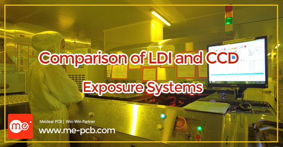
In the PCB (Printed Circuit Board) manufacturing process, exposure is a critical step. Many PCB manufacturers like meidearpcb utilize CCD semi-automatic exposure machines for this process.

LED lighting PCB (Printed Circuit Board) Solutions
Jan .01.2025
LED lighting PCB (Printed Circuit Board) solutions
CEM-3 Thermal conductive material
IMS pcb Flexible pcb Copper-base pcbs
CEM-3 Thermal conductive material
IMS pcb Flexible pcb Copper-base pcbs


